Dream diodes with a graphene interlayer
Advertisement


A team of researchers, affiliated with UNIST has created a new technique that greatly enhances the performance of Schottky diodes (metal-semiconductor junction) used in electronic devices. Their research findings have attracted considerable attention within the scientific community by solving the contact resistance problem of metal-semiconductor, which had remained unsolved for almost 50 years.
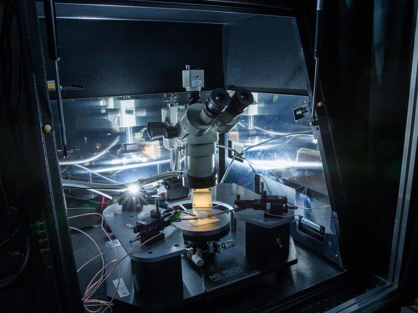
Shown above is the Internal Photoemission (IPE) Measurement System, developed by Hoon Hahn Yoon, combined M.S./Ph.D. student of Natural Science at UNIST.
UNIST
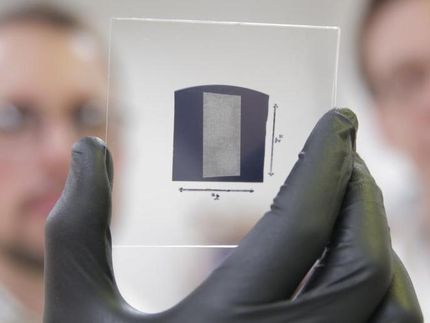
The researchers have created a new type of diode with a graphene insertion layer sandwiched between metal and semiconductor. This new technique blows all previous attemps out the water, as it is expected to significantly contribute to the semiconductor industry's growth.
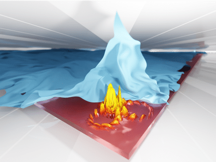
The Schottky diode is one of the oldest and most representative semiconductor devices, formed by the junction of a semiconductor with a metal. However, due to the atomic intermixing along the interface between two materials, it has been impossible to produce an ideal diode. (An ideal diode acts like a perfect conductor when voltage is applied forward biased and like a perfect insulator when voltage is applied reverse biased.)
Professor Kibog Park of Natural Science solved this problem by inserting a graphene layer at the metal-semiconductor interface. In the study, the research team demonstrated that this graphene layer, consisting of a single layer of carbon atoms can not only suppress the material intermixing substantially, but also matches well with the theoretical prediction.
"The sheets of graphene in graphite have a space between each sheet that shows a high electron density of quantum mechanics in that no atoms can pass through," says Professor Park. "Therefore, with this single-layer graphene sandwiched between metal and semiconductor, it is possible to overcome the inevitable atomic diffusion problem."
The study also has the physiological meaning of confirming the theoretical prediction that "In the case of silicon semiconductors, the electrical properties of the junction surfaces hardly change regardless of the type of metal they use," according to Hoon Hahn Yoon (Combined M.S./Ph.D. student of Natural Science), the first author of the study.
The internal photoemission method was used to measure the electronic energy barrier of the newly-fabricated metal/graphene/n-Si(001) junction diodes. The Internal Photoemission (IPE) Measurement System in the image shown above has contributed greatly to these experiments. This system has been developed by four UNIST graduate students (Hoon Han Yoon, Sungchul Jung, Gahyun Choi, and Junhyung Kim), which was carried out as part of an undergraduate research project in 2012 and was supported by the Korea Foundation for the Advancement of Science and Creativity (KOFAC).
"Students have teamed up and carried out all the necessary steps for the research since they were undergraduates," Professor Park says. "Therefore, this research is a perfect example of time, persistence, and patience paying off."
Original publication
Hoon Hahn Yoon, Sungchul Jung, Gahyun Choi, Junhyung Kim, Youngeun Jeon, Yong Soo Kim, Hu Young Jeong, Kwanpyo Kim, Soon-Yong Kwon, and Kibog Park; "Strong Fermi-Level Pinning at Metal/n-Si(001) Interface Ensured by Forming an Intact Schottky Contact with a Graphene Insertion Layer"; Nano Letters; 2017


Other news from the department science


