Development of Nanoscale Superlattice Structures and Nanodevices
Advertisement


Harvard University Professor and Nanosys Co-Founder Charlie Lieber Raises the Stakes in the Development of Nanoscale Superlattice Structures and Nanodevices --------------------------------------------------------------------------------
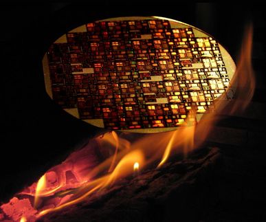
CAMBRIDGE, Mass., -- Nanosys Incorporated announced the publication of a landmark paper in the February 7, 2002 issue of Nature. Dr. Charles Lieber, Nanosys Co-founder and the Mark Hyman Professor of Chemistry of Harvard University, authored the paper along with his graduate students Mark Gudiksen, Lincoln Lauhon, Jianfang Wang, and David Smith. The paper -- which is entitled ``Growth of Nanowire Superlattice Structures for Nanoscale Photonics and Electronics'' -- demonstrates general methods for controlling the composition and charge of multiple materials on a single nanostructure. The researchers take advantage of the flexible control of multiple variables to build novel devices in electronics, photonics, and opto-electronics. Lieber's work is the first example of a generic method for creating heterojunctions of arbitrary materials in a single nanostructure. In addition, Lieber's technique allows the modulation of doping levels along the length of a single nanowire. This ability to control charge and composition on the nanoscale enabled the Lieber group to make a variety of unique prototype devices such as GaAs emitters embedded in GaP wires, novel n-Si/p-Si nanowire diodes for high density nano-scale logic, and nanometer sized LEDs derived from alternating segments of n-InP/p-InP on a single nanowire. This robust synthetic method allows for the creation of superlattice heterostructures of materials that cannot be interfaced in macroscopic structures. This could open the door to the discovery of new materials and devices for a semiconductor industry that faces the impending limit to Moore's law. The new process developed in the Lieber laboratory allows two different materials to be placed next to each other on the same nanometer-sized semiconductor crystal in a manner that creates a perfect electrical junction (defect-free). The Nature paper showcases the power of this technology by developing several novel prototype devices enabled by these new materials.
In the first set of experiments, the researchers controlled the growth of segments of light emitting GaAs spaced by non-emitting GaP segments on a single nanowire. These nanowires functioned as photonic devices with emission of light from the GaAs segments only when excitation light was directed along the nanowire. In addition to controlling the incorporation of different materials, the group of researchers also demonstrated that the length of each segment could be controlled precisely. By varying the lengths of the GaP and GaAs segments, a nano-barcode was created that could be read by measuring the pattern of the fluorescence along the length of the wire. Just like a grocery-store barcode, in which a pattern of different-thickness lines is used to uniquely identify an item, these unique structures could potentially form the basis for a nano-encoding system. Other applications of this type of precise control fall in areas of photonics, electronics and quantum computing.
The general methodology of placing materials with different bandgaps in precise contact offers additional benefits, such as the ability to create individual wires with specifically engineered bandgaps. Other potential applications include the creation of both one-dimensional waveguides that are formed from the emitting material, and intrinsic cavities for nanowire lasers.
Finally, the researchers were able to use their new technology to create the most essential element in modern electronics within a single nanowire: a p-n junction. In this demonstration, the researchers fabricated a batch of nanowires that were composed of half p-type silicon, half n-type silicon. The resulting interface produced a functional p-n junction on the nanoscale. In addition to applications in nanoelectronics, such as bipolar transistors and highly integrated nano-logic arrays, such devices could play a role in the creation of ultra-sensitive biological and chemical sensors for the detection of biowarfare agents among other sensing targets. P-n junctions in InP nanowires were also formed to create a single nanowire LED device. Potential applications for a single nanowire LED include quantum cryptography and information processing. The ability to control charge in a binary format may lead to creative methods of designing assemblies of different nanowires to arrive at complex architectures.
``This work really sets our technology apart in the creation of superlattice structures that are varied by materials, doping modulation, and segment size control in heterostructures. In addition the excellent graduate students in my lab extended this basic materials development advance into the proof-of-concept stage by building three completely novel device applications in photonics, electronics, and opto-electronics. At the moment our laboratory is in the enviable position of deciding which type of new device to make, as the possibilities for materials development and device applications seem almost infinite at this point in time,'' said Professor Lieber.
``I am awestruck by how rapidly the development of nanowire technology is occurring. The Lieber technology and materials are truly a once in a lifetime advance that will only be completely appreciated once Nanosys translates this excellent scientific work into equally impressive products in the electronics, opto-electronics, and molecular sensing markets. The range of applications will force us to make some important decisions in terms of what technologies to develop internally and what applications to develop with partner companies,'' said Nanosys President and CEO, Larry Bock.
About Professor Charles Lieber
Dr. Lieber is a Scientific Founder of Nanosys, Inc., a Member of the Board of Directors, and Chairman of the Scientific Advisory Board. Dr. Lieber is the Mark Hyman Professor of Chemistry at Harvard University. Dr. Lieber is the world's leading authority on the synthesis of one-dimensional, nano-structured materials (nanowires), and on the design of nanowire enabled devices. Dr. Lieber's laboratory is able to rationally design, control and scale the first robust building blocks of nanoscale device architecture. His laboratory has created prototypes for nano-scale devices with biological, electronic and optoelectronic applications. Dr. Lieber has won numerous awards including the Feynman Prize for Nanotechnology, the Creativity Award of the National Science Foundation, the Leo Hendrik Baekeland Award from the American Chemical Society, the Materials Research Society Outstanding Young Investigator Award, and the Presidential Young Investigators Award. Dr. Lieber graduated with a Ph.D. in Chemistry from Stanford University and carried out his Post Doctoral work at the California Institute of Technology. Prior to taking his position at Harvard, Dr. Lieber was a Professor of Chemistry at Columbia University.
About Nanosys
Nanosys, Inc. is a newly formed company focused on the development of nanotechnology-enabled systems. These systems incorporate novel and patent-protected zero and one-dimensional nanometer-scale materials such as nanowires, nanotubes and nanodots (quantum dots) as their principal active elements. These systems exploit the fundamentally unique electronic, magnetic, optical and integration properties associated with materials having nanometer-scale dimensions. Devices constructed with these systems will revolutionize a broad array of industries from chemical sensing to nanoelectronics (electronic memory and logic) to opto-electronics. These devices will offer radical performance gains in speed, sensitivity, power consumption, device density, and integration.


Other news from the department science


These products might interest you


Most read news


More news from our other portals


See the theme worlds for related content
Topic world Sensor technology
Sensor technology has revolutionized the chemical industry by providing accurate, timely and reliable data across a wide range of processes. From monitoring critical parameters in production lines to early detection of potential malfunctions or hazards, sensors are the silent sentinels that ensure quality, efficiency and safety.
Topic world Synthesis
Chemical synthesis is at the heart of modern chemistry and enables the targeted production of molecules with specific properties. By combining starting materials in defined reaction conditions, chemists can create a wide range of compounds, from simple molecules to complex active ingredients.