To use all functions of this page, please activate cookies in your browser.
My watch list
my.chemeurope.com
my.chemeurope.com
With an accout for my.chemeurope.com you can always see everything at a glance – and you can configure your own website and individual newsletter.
- My watch list
- My saved searches
- My saved topics
- My newsletter
Scanning tunneling microscope
Scanning tunneling microscopy (STM) is a powerful technique for viewing surfaces at the atomic level. Its development in 1981 won its inventors, Gerd Binnig and Heinrich Rohrer (at IBM Zürich), the Nobel Prize in Physics in 1986 [1]. STM probes the density of states of a material using tunneling current. For STM, good resolution is considered to be 0.1 nm lateral resolution and 0.01 nm depth resolution [2]. The STM can be used not only in ultra high vacuum but also in air and various other liquid or gas ambients, and at temperatures ranging from near 0 kelvins to a few hundred degrees Celsius [3]. The STM is based on the concept of quantum tunneling. When a conducting tip is brought very near to a metallic or semiconducting surface, a bias between the two can allow electrons to tunnel through the vacuum between them. For low voltages, this tunneling current is a function of the local density of states (LDOS) at the Fermi level, Ef, of the sample [3]. Variations in current as the probe passes over the surface are translated into an image. STM can be a challenging technique, as it requires extremely clean surfaces and sharp tips. Product highlight
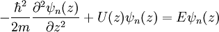
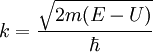
TunnelingTunneling is a concept that arises from quantum mechanics. Classically, an object hitting an impenetrable wall of infinite height will bounce back. Imagine throwing a baseball to a friend on the other side of a mile high brick wall, directly at the wall. One would be rightfully astonished if, rather than bouncing back upon impact, the ball were to simply pass through to your friend on the other side of the wall. For objects of very small mass, as is the electron, wavelike nature has a more pronounced effect, so such an event, referred to as tunneling, has a much greater probability. This section refers heavily to C. Julian Chen’s Introduction to Scanning Tunneling Microscopy, listed as reference [3]. Electrons behave as waves of energy, and in the presence of a potential U(z), assuming 1-dimensional case, the energy levels ψn(z) of the electrons are given by solutions to Schrödinger’s equation,
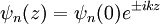
where ħ is Planck’s constant, z is the position, and m is the mass of an electron [3]. If an electron of energy E is incident upon an energy barrier of height U(z), the electron wave function is a traveling wave solution,
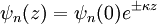
where if E > U(z), which is true for a wave function inside the tip or inside the sample [3]. Inside a barrier, such as between tip and sample, E < U(z) so the wave functions which satisfies this are decaying waves,
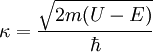
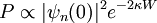
where quantifies the decay of the wave inside the barrier, with the barrier in the +z direction for − κ [3]. Knowing the wave function allows one to calculate the probability density for that electron to be found at some location. In the case of tunneling, the tip and sample wave functions overlap such that when under a bias, there is some finite probability to find the electron in the barrier region and even on the other side of the barrier [3]. Let us assume the bias is V and the barrier width is W, as illustrated in Figure 1. This probability, P, that an electron at z=0 (left edge of barrier) can be found at z=W (right edge of barrier) is proportional to the wave function squared,
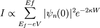
If the bias is small, we can let U − E ≈ φM in the expression for κ, where φM, the work function, gives the minimum energy needed to bring an electron from an occupied level, the highest of which is at the Fermi level (for metals at T=0 kelvins), to vacuum level. When a small bias V is applied to the system, only electronic states very near the Fermi level, within eV, are excited [3]. These excited electrons can tunnel across the barrier. In other words, tunneling occurs mainly with electrons of energies near the Fermi level. However, tunneling does require that there is an empty level of the same energy as the electron for the electron to tunnel into on the other side of the barrier. It is because of this restriction that the tunneling current can be related to the density of available or filled states in the sample. The current due to an applied voltage V (assume tunneling occurs sample to tip) depends on two factors: 1) the number of electrons between Ef and eV in the sample, and 2) the number among them which have corresponding free states to tunnel into on the other side of the barrier at the tip [3]. The higher density of available states the greater the tunneling current. When V is positive, electrons in the tip tunnel into empty states in the sample; for a negative bias, electrons tunnel out of occupied states in the sample into the tip [3]. Mathematically, this tunneling current is given by
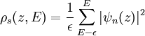
One can sum the probability over energies between Ef − eV and eV to get the number of states available in this energy range per unit volume, thereby finding the local density of states (LDOS) near the Fermi level [3]. The LDOS near some energy E in an interval ε is given by
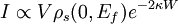
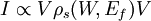
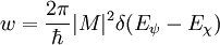
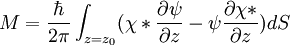
and the tunnel current at a small bias V is proportional to the LDOS near the Fermi level, which gives important information about the sample [3]. It is desirable to use LDOS to express the current because this value does not change as the volume changes, while probability density does [3]. Thus the tunneling current is given by where ρs(0,Ef) is the LDOS near the Fermi level of the sample at the sample surface [3]. By using equation (6), this current can also be expressed in terms of the LDOS near the Fermi level of the sample at the tip surface, The exponential term in (9) is very significant in that small variations in W greatly influence the tunnel current. If the separation is decreased by 1 Ǻ, the current increases by an order of magnitude, and vice versa [4]. This approach fails to account for the rate at which electrons can pass the barrier. This rate should affect the tunnel current, so it can be accounted for by using Fermi’s Golden Rule with the appropriate tunneling matrix element. John Bardeen solved this problem in his study of the metal-insulator-metal junction, MIM [5]. He found that if he solved Schrödinger’s equation for each side of the junction separately to obtain the wave functions ψ and χ for each electrode, he could obtain the tunnel matrix, M, from the overlap of these two wave functions [3]. This can be applied to STM by making the electrodes the tip and sample, assigning ψ and χ as sample and tip wave functions, respectively, and evaluating M at some surface S between the metal electrodes at z=zo, where z=0 at the sample surface and z=W at the tip surface [3]. Now, Fermi’s Golden Rule gives the rate for electron transfer across the barrier, and is written
where δ(Eψ-Eχ) restricts tunneling to occur only between electron levels with the same energy [3]. The tunnel matrix element, given by
is a description of the lower energy associated with the interaction of wave functions at the overlap, also called the resonance energy [3]. Summing over all the states gives the tunneling current as
where f is the Fermi function, ρs and ρT are the density of states in the sample and tip, respectively [3]. The Fermi distribution function describes the filling of electron levels at a given temperature T. ProcedureFirst the tip is brought into close proximity of the sample by some coarse sample-to-tip control. The values for common sample-to-tip distance, W, range from about 4-7 Ǻ, which is the equilibrium position between attractive (3 In constant current mode, feedback electronics adjust the height by a voltage to the piezoelectric height control mechanism [6]. This leads to a height variation and thus the image comes from the tip topography across the sample and gives a constant charge density surface; this means contrast on the image is due to variations in charge density [4]. In constant height, the voltage and height are both held constant while the current changes to keep the voltage from changing; this leads to an image made of current changes over the surface, which can be related to charge density [4]. The benefit to using a constant height mode is that it is faster, as the piezoelectric movements require more time to register the change in constant current mode than the voltage response in constant height mode [4]. In addition to scanning across the sample, information on the electronic structure of the sample can be obtained by sweeping voltage and measuring current at a specific location [2]. This type of measurement is called scanning tunneling spectroscopy (STS). InstrumentationThe components of an STM include scanning tip, piezoelectric controlled height and x,y scanner, coarse sample-to-tip control, vibration isolation system, and computer [6]. The resolution of an image is limited by the radius of curvature of the scanning tip of the STM. Additionally, image artifacts can occur if the tip has two tips at the end rather than a single atom; this leads to “double-tip imaging,” a situation in which both tips contribute to the tunneling [2]. Therefore it has been essential to develop processes for consistently obtaining sharp, usable tips. Recently, carbon nanotubes have been used in this instance. The tip is often made of tungsten or platinum-iridium, though gold is also used [2]. Tungsten tips are usually made by electrochemical etching, and platinum-iridium tips by mechanical shearing [2]. Both processes are outlined in C. Bai’s book, reference [2] below. Due to the extreme sensitivity of tunnel current to height, proper vibration isolation is imperative for obtaining usable results. In the first STM by Binnig and Rohrer, magnetic levitation was used to keep the STM free from vibrations; now spring systems are often used [3]. Additionally, mechanisms for reducing eddy currents are implemented. Maintaining the tip position with respect to the sample, scanning the sample in raster fashion and acquiring the data is computer controlled [6]. The computer is also used for enhancing the image with the help of image processing as well as performing quantitative morphological measurements. Other STM Related StudiesMany other microscopy techniques have been developed based upon STM. These include Photon Scanning Tunneling Microscopy (PSTM), which uses an optical tip to tunnel photons [2]; Scanning Tunneling Potentiometry (STP), which measures electric potential across a surface [2]; and spin polarized scanning tunneling microscopy (SPSTM), which uses a ferromagnetic tip to tunnel spin-polarized electrons into a magnetic sample [7]. Other STM methods involve manipulating the tip in order to change the topography of the sample. This is attractive for several reasons. Firstly the STM has an atomically precise positioning system which allows very accurate atomic scale manipulation. Furthermore, after the surface is modified by the tip, it is a simple matter to then image with the same tip, without changing the instrument. IBM researchers developed a way to manipulate Xenon atoms adsorbed on a nickel surface [2] This technique has been used to create electron "corrals" with a small number of adsorbed atoms, which allows the STM to be used to observe electron Friedel Oscillations on the surface of the material. Aside from modifying the actual sample surface, one can also use the STM to tunnel electrons into a layer of E-Beam photoresist on a sample, in order to do lithography. This has the advantage of offering more control of the exposure than traditional Electron beam lithography. Recently groups have found they can use the STM tip to rotate individual bonds within single molecules. The electrical resistance of the molecule depends on the orientation of the bond, so the molecule effectively becomes a molecular switch. References
See alsoWikibooks' [[wikibooks:|]] has more about this subject:
The Opensource Handbook of Nanoscience and Nanotechnology
Literature
|
|||||||||||||||||||||||
| This article is licensed under the GNU Free Documentation License. It uses material from the Wikipedia article "Scanning_tunneling_microscope". A list of authors is available in Wikipedia. | |||||||||||||||||||||||

 ,
,
 ,
,
 ,
,
 .
.
 ,
,
 ,
,
 ,
,
![I = \frac{4 \pi e}{\hbar}\int_{-\infty}^{+\infty} [f(E_f -eV) - f(E_f + \epsilon)] \rho_s (E_f - eV + \epsilon) \rho_T (E_f + \epsilon)|M|^2 d \epsilon](images/math/0/3/5/03500fca9e755383ae080907a59f41cd.png) ,
,
Last viewed


