Precision landing in the atomic lattice - new ways to improve catalysis and gas detection
Innovative combination of methods allows precise localization of individual atoms in ultra-thin materials

Advertisement


A research team from the University of Vienna and Vienna University of Technology has succeeded in incorporating individual platinum atoms into an ultra-thin material in a targeted manner - and for the first time, has been able to demonstrate with atomic precision which position they occupy in the lattice. This was made possible by a newly developed combination of methods involving the creation of defects in the carrier material, the controlled incorporation of individual platinum atoms and a particularly high-contrast electron imaging process ("ptychography"). The work, published in the journal Nano Letters, provides new approaches for targeted material modification.
In order to make materials particularly efficient for applications such as catalysis (acceleration of chemical reactions) or the detection of certain gases, they have to be modified at an atomic level. So-called active centers - tiny spots on the surface of the material where chemical reactions take place or gas molecules can dock in a targeted manner - are crucial here. Such centers are particularly effective if they consist of individual metal atoms, such as platinum. The aim of the current study was therefore to produce this type of material - and at the same time to make its structure visible at an atomic level.
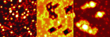
A sharp look into the atomic lattice
Molybdenum disulphide (MoS2), an ultra-thin semiconductor that is characterized by its good modifiability, was used as the carrier material. To create space for new active centers, the research team used helium ion bombardment to create microscopic defects ("defect engineering") in the MoS₂ surface - e.g. sulphur gaps - and then filled these with individual platinum atoms. This controlled exchange of atoms in the lattice ("doping") can be used to specifically change the properties of materials.
Until now, however, there has been a lack of precise evidence of exactly where the introduced foreign atoms are located in the atomic lattice, as different types of defects - such as single or double sulphur gaps - can hardly be distinguished using conventional electron microscopy due to the low contrast. The researchers therefore relied on "single-sideband ptychography" (SSB), a state-of-the-art imaging method based on the evaluation of electron diffraction patterns. First author of the study David Lamprecht, who started the research at the University of Vienna and is now continuing it at the Institute of Microelectronics at TU Wien, explains: "With our combination of defect engineering, doping and ptychography, we have succeeded in making even subtle differences in the atomic lattice visible - and clearly proving whether a platinum atom has actually been built into a gap or is just sitting loosely on the surface." With the help of computer simulations, it was possible to precisely identify the various installation sites (e.g. sulphur or molybdenum sites) - a decisive step for targeted material design.
Two applications, one atom
The combination of targeted incorporation and atom-precise imaging opens up new possibilities for two key future fields: Catalysis and gas sensing. Individual platinum atoms at precisely defined locations can act as particularly efficient catalysts - for example in environmentally friendly hydrogen production. At the same time, the material can be tailored so that it only reacts to certain gas molecules. "With this control over the installation sites, we can selectively develop functionalized sensors - a significant improvement over existing methods," emphasizes Jani Kotakoski, last author and research group leader at the Faculty of Physics at the University of Vienna.
Building blocks for functional materials
The combination of methods presented can be applied not only to platinum and MoS2, but in principle to many other combinations of 2D materials and dopant atoms. In the future, the approach is to be further developed - for example through finer control of defect formation or additional post-treatments. The aim is to develop functional materials with tailored properties in which every single atom is in the right place.
Note: This article has been translated using a computer system without human intervention. LUMITOS offers these automatic translations to present a wider range of current news. Since this article has been translated with automatic translation, it is possible that it contains errors in vocabulary, syntax or grammar. The original article in German can be found here.
Original publication


Other news from the department science


