To use all functions of this page, please activate cookies in your browser.
My watch list
my.chemeurope.com
my.chemeurope.com
With an accout for my.chemeurope.com you can always see everything at a glance – and you can configure your own website and individual newsletter.
- My watch list
- My saved searches
- My saved topics
- My newsletter
CeramographyCeramography is the art and science of preparation, examination and evaluation of ceramic microstructures.[1] Ceramography can be thought of as the metallography of ceramics, and falls under the Structure heading of the materials science tetrahedron. The microstructure is the structure level of approximately 0.1 to 100 µm, between the minimum wavelength of visible light and the resolution limit of the naked eye. The microstructure includes most grains, secondary phases, grain boundaries, pores, micro-cracks and hardness microindentions. Most bulk mechanical, optical, thermal, electrical and magnetic properties are significantly affected by the microstructure. The fabrication method and process conditions are generally indicated by the microstructure. The root cause of many ceramic failures is evident in the microstructure. Ceramography is part of the broader field of materialography, which includes all the microscopic techniques of material analysis, such as metallography, petrography and plastography. Ceramography is usually reserved for high-performance ceramics for industrial applications, such as 85-99.8% alumina (Al2O3), zirconia (ZrO2), silicon carbide (SiC), silicon nitride (Si3N4), and ceramic-matrix composites. It is seldom used on porcelain sanitary fixtures or decorative and commodity ceramics such as dishes and pottery. Product highlight
A Brief History of CeramographyCeramography evolved along with other branches of materialography. Alois de Widmanstätten of Austria etched a meteorite in 1808 to reveal proeutectoid ferrite bands that grew on prior austenite grain boundaries. Geologist Henry Clifton Sorby, the "father of metallography," applied petrographic techniques to the steel industry in the 1860s in Sheffield, England. French geologist Auguste Michel-Lévy devised a chart that correlated the optical properties of minerals to their polarization color and thickness in the 1880s. Swedish metallurgist J.A. Brinell invented the first quantitative hardness scale in 1900. R.L. Smith and G.E. Sandland developed the first microindention hardness test at Vickers Ltd. in London in 1922.[2] Swiss-born microscopist A.I. Buehler started the first metallographic equipment manufacturer near Chicago in 1936. Frederick Knoop and colleagues at the National Bureau of Standards developed a less-penetrating (than Vickers) microindention test in 1939.[3] G.L. Kehl of Columbia University wrote The Principles of Metallographic Laboratory Practice in 1949, a book that was considered the bible of materialography until the 1980s. Kehl co-founded a group within the Atomic Energy Commission that became the International Metallographic Society in 1967. Preparation of Ceramographic SpecimensThe preparation of ceramic specimens for microstructural analysis consists of five broad steps: sawing, embedding, grinding, polishing and etching. The tools and consumables for ceramographic preparation are available worldwide from metallography equipment vendors and laboratory supply companies.
Alternatively, non-cubic ceramics can be prepared as thin sections, also known as petrography, for examination by polarized transmitted light microscopy. In this technique, the specimen is sawed to ~1 mm thick, glued to a microscope slide, and ground to a thickness (x) approaching 30 µm. A cover slip is glued onto the exposed surface. The adhesives, such as epoxy or Canada balsam resin, must have approximately the same refractive index (η ≈ 1.54) as glass. Most ceramics have a very small absorption coefficient (α ≈ 0.5 cm-1 for alumina) in the Beer-Lambert law below, and can be viewed in transmitted light. Cubic ceramics, e.g. yttria-stabilized zirconia and spinel, have the same refractive index in all crystallographic directions and are, therefore, opaque when the microscope's polarizer is 90° out of phase with its analyzer.
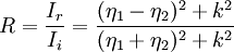
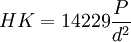
Ceramographic specimens are electrical insulators in most cases, and must be coated with a conductive ~10-nm layer of metal or carbon for electron microscopy, after polishing and etching. Gold or Au-Pd alloy from a sputter coater or evaporative coater also improves the reflection of visible light from the polished surface under a microscope, by the Fresnel formula below. Bare alumina (η ≈ 1.77, k ≈ 10-6) has a negligible extinction coefficient and reflects only 8% of the incident light from the microscope. Gold-coated (η ≈ 0.82, k ≈ 1.59 @ λ = 500 nm) alumina reflects 44% in air, 39% in immersion oil. Ceramographic AnalysisCeramic microstructures are most often analyzed by reflected visible-light microscope in brightfield. Darkfield is used in limited circumstances, such as to reveal cracks. Polarized transmitted light is used with thin sections, where the contrast between grains comes from birefringence. Very fine microstructures may require the higher magnification and resolution of a scanning electron microscope (SEM) or confocal laser scanning microscope (CLSM). The cathodoluminescence microscope (CLM) is useful for distinguishing phases of refractories. The transmission electron microscope (TEM) and scanning acoustic microscope (SAM) have specialty applications in ceramography. Ceramography is often done qualitatively, for comparison of the microstructure of a component to a standard for quality control or failure analysis purposes. Three common quantitative analyses of microstructures are grain size, second-phase content and porosity. Microstructures are measured by the principles of stereology, in which three-dimensional objects are evaluated in 2-D by projections or cross-sections. Grain size can be measured by the line-fraction or area-fraction methods of ASTM E112. In the line-fraction methods, a statistical grain size is calculated from the number of grains or grain boundaries intersecting a line of known length or circle of known circumference. In the area-fraction method, the grain size is calculated from the number of grains inside a known area. In each case, the measurement is affected by secondary phases, porosity, preferred orientation, exponential distribution of sizes, and non-equiaxed grains. Image analysis can measure the diameter(s) and shape factors of individual grains by ASTM E1382. Second-phase content and porosity are measured the same way in a microstructure, such as ASTM E562. E562 is a point-fraction method based on the stereological principle of point fraction = volume fraction, i.e., Pp = Vv. Second-phase content in ceramics, such as carbide whiskers in an oxide matrix, is usually expressed as a mass fraction. Volume fractions can be converted to mass fractions if the density of each phase is known. Image analysis can measure porosity, pore-size distribution and volume fractions of secondary phases by ASTM E1245. Porosity measurements do not require etching. Multi-phase microstructures do not require etching if the contrast between phases is adequate, as is usually the case. Grain size, porosity and second-phase content have all been correlated with ceramic properties such as mechanical strength σ by the Hall-Petch equation, hardness, toughness, dielectric constant and many others. Microindention Hardness and ToughnessThe hardness of a material can be measured in many ways. The Knoop hardness test, a method of microindention hardness, is the most reproducible for dense ceramics. The Vickers hardness test and superficial Rockwell scales (e.g., 45N) can also be used, but tend to cause more surface damage than Knoop. The Brinell test is suitable for ductile metals, but not ceramics. In the Knoop test, a diamond indenter in the shape of an elongated pyramid is forced into a polished (but not etched) surface under a predetermined load, typically 500 or 1000 gm. The load is held for some amount of time, say 10 s, and the indenter is retracted. The indention long diagonal (d, μm) is measured under a microscope, and the Knoop hardness (HK) is calculated from the load (P, gm) and the square of the diagonal length in the equations below. Most oxide ceramics have a Knoop hardness in the range of 1000 - 1500 kgf/mm2 (10 - 15 GPa), and many carbides are over 2000 (20 GPa). The method is specified in ASTM C849, C1326 & E384. Microindention hardness is also called microindentation hardness or simply microhardness.
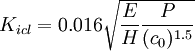
The toughness of ceramics can be determined from a Vickers test under a load of 10 - 20 kg. Toughness is the ability of a material to resist crack propagation. Several calculations have been formulated from the load (P), elastic modulus (E), microindention hardness (H), crack length (c) and flexural strength (σ). Modulus of rupture (MOR) bars with a rectangular cross-section are indented in three places on a polished surface. The bars are loaded in 4-point bending with the polished, indented surface in tension, until fracture. The fracture normally originates at one of the indentions. The crack lengths are measured under a microscope. The toughness of most ceramics is 2-4 MPa√m, but toughened zirconia is as much as 13, and cemented carbides are often over 20.[4]
Further Reading
References
Categories: Metallurgy | Materials science |
|
| This article is licensed under the GNU Free Documentation License. It uses material from the Wikipedia article "Ceramography". A list of authors is available in Wikipedia. |


 and
and 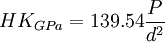
 initial crack length
![K_{isb} = 0.59 \left(\frac{E}{H}\right)^{1/8}[\sigma (P^{1/3})]^{3/4}](images/math/d/8/f/d8f42b589951b688dd7c47d2b7704d0b.png) indention strength in bending
indention strength in bending


