From crystal to new 2D materials space
New method enables the study of nanostructures beyond classic layered systems
Advertisement


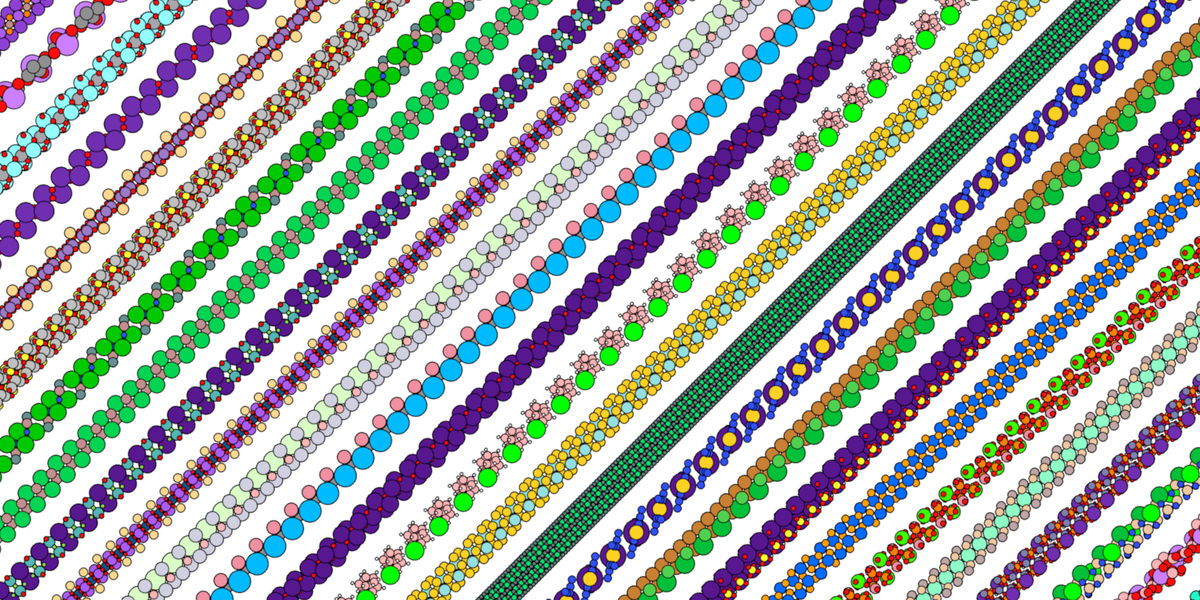
Two-dimensional materials can exhibit properties that do not occur in their three-dimensional parent systems, making them particularly interesting for applications in electronics, for example. So far, the search mainly concentrated on crystals that were already composed of loosely bonded layers. For the first time, a team at the Helmholtz-Zentrum Dresden-Rossendorf (HZDR) and TU Dresden has now developed an efficient computational method that predicts separable atomic layers in any type of crystal. By analyzing more than 24,000 known crystal structures, they identified 2,531 particularly promising candidates. The findings have been published in Nature Communications.
Since the production of graphene in 2004, two-dimensional materials have been sparking great scientific and technological interest. As they are only a few atomic layers thick, or even just a single atomic layer, they can exhibit special electronic, magnetic or chemical properties – which make them particularly interesting for applications such as electronics, catalysis and energy storage.
The best-known examples are formed from so-called van der Waals crystals. Just like a book, they are composed of individual layers held together by comparatively weak forces. It is therefore relatively easy to peel off individual layers. In non-layered crystals, on the other hand, the atoms form a three-dimensional network of significantly stronger bonds. Until now, it has been difficult to predict which of these solids could be split into stable layers.
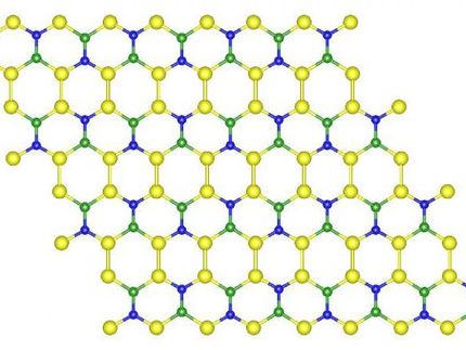
“Given that this class of materials is still so young, selecting suitable materials for experiments was often based on experience and intuition,” explains Dr. Rico Friedrich of HZDR’s Institute of Ion Beam Physics and Materials Research and TU Dresden. “Using our universal method, we can now determine the points at which a crystal in any material can best be split and whether a potentially stable two-dimensional structure can form in the process.”
Bond strengths instead of mere distances
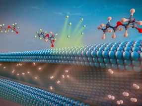
The core of the new approach is the eXfoliation and Cleavage Potential, or XCP, for short. The computational model uses the chemical elements involved and the distance between them to calculate very precisely the strength of the bonds between individual atoms. Two additional algorithms subsequently search either for easily separable crystal planes or gradually remove the weakest bonds from the model until two-dimensional substructures remain. By doing so, the method also detects atomically uneven separation surfaces.
“Calculating the electronic structure for every conceivable surface would be incredibly time-consuming,” says the lead author, Tom Barnowsky. “Our efficient model, on the other hand, can search big materials databases with minimal computational effort. Detailed calculations are only required for particularly promising hits.”
Wide-ranging tests on two-dimensional materials already produced experimentally have shown that the XCP method can reliably determine the preferred exfoliable planes. It is also freely available to interested parties as a web tool ( http://xcp.hzdr.de/ ).
Thousands of promising structures
The team applied the method to more than 24,000 known, non-layered crystal structures from one of the largest experimental materials databases. Of those, the researchers chose 2,531 particularly promising candidates for more precise calculations. In these materials, the chemical composition remains unchanged upon detachment, while the calculated bonding ratios strongly favor the formation of a two-dimensional structure.
Further investigations confirmed the selection’s potential: in most of the candidates the team calculated comparatively low exfoliation energies. Moreover, many of the structures proved both dynamically and thermodynamically stable – a basic precondition for technological applications. Now the experiments have to demonstrate whether and under what conditions they can actually be produced.
The predicted 2D materials differ markedly from the existing database entries. Some might even undergo a fundamental change in their electronic properties during the transition to a thin layer: among other things, the calculations predict compounds in which the three-dimensional crystals act as semiconductors while becoming metallic in two dimensions. In others, a direct band gap is created, which may be of interest for optoelectronic devices. Magnetic candidates could also open up new possibilities for spintronics in data processing and storage.
“Our results vastly expand the horizon for two-dimensional materials,” summarizes Friedrich. “The method doesn’t guarantee that every candidate can be produced in the lab. But it does show which crystals are actually worth the experimental effort.”
Original publication


Other news from the department science