To use all functions of this page, please activate cookies in your browser.
My watch list
my.chemeurope.com
my.chemeurope.com
With an accout for my.chemeurope.com you can always see everything at a glance – and you can configure your own website and individual newsletter.
- My watch list
- My saved searches
- My saved topics
- My newsletter
Electronic band structureIn solid state physics, the electronic band structure (or simply band structure) of a solid describes ranges of energy that an electron is "forbidden" or "allowed" to have. It is due to the diffraction of the quantum mechanical electron waves in the periodic crystal lattice. The band structure of a material determines several characteristics, in particular its electronic and optical properties. Product highlight
Why bands occurThe electrons of a single free-standing atom occupy atomic orbitals, which form a discrete set of energy levels. If several atoms are brought together into a molecule, their atomic orbitals split like in a coupled oscillation. This produces a number of molecular orbitals proportional to the number of atoms. When a large number of atoms (of order 1020 or more) are brought together to form a solid, the number of orbitals becomes exceedingly large, and the difference in energy between them becomes very small, so the levels form bands of energy rather than the discrete energy levels of the atoms in isolation. However, some intervals of energy contain no orbitals, no matter how many atoms are aggregated, forming band gaps. Within an energy band, energy levels are so numerous as to be a near continuum. First, the separation between energy levels in a solid is comparable with the energy that electrons constantly exchange with phonons (atomic vibrations). Second, it is comparable with the energy uncertainty due to the Heisenberg uncertainty principle, for reasonably long intervals of time. As a result, the separation between energy levels is of no consequence. Several approaches to finding band structure are discussed below Basic conceptsAny solid has a large number of bands. In theory, it can be said to have infinitely many bands (just as an atom has infinitely many energy levels). However, all but a few lie at energies so high that any electron that reaches those energies escapes from the solid. These bands are usually disregarded. Bands have different widths, based upon the properties of the atomic orbitals from which they arise. Also, allowed bands may overlap, producing (for practical purposes) a single large band. Metals contain a band that is partly empty and partly filled regardless of temperature. Therefore they have very high conductivity. The uppermost occupied band in an insulator or semiconductor is called the valence band by analogy to the valence electrons of individual atoms. The lowermost unoccupied band is called the conduction band because only when electrons are excited to the conduction band can current flow in these materials. The difference between insulators and semiconductors is only that the forbidden band gap between the valence band and conduction band is larger in an insulator, so that fewer electrons are found there and the electrical conductivity is less. Because one of the main mechanisms for electrons to be excited to the conduction band is due to thermal energy, the conductivity of semiconductors is strongly dependent on the temperature of the material. This band gap is one of the most useful aspects of the band structure, as it strongly influences the electrical and optical properties of the material. Electrons can transfer from one band to the other by means of carrier generation and recombination processes. The band gap and defect states created in the band gap by doping can be used to create semiconductor devices such as solar cells, diodes, transistors, laser diodes, and others. A more complete view of the band structure takes into account the periodic nature of a crystal lattice. The Schrödinger equation is solved for the crystal, which has Bloch waves as solutions:
where k is called the wavevector, and is related to the direction of motion of the electron in the crystal, and n is the band index, which simply numbers the energy bands. The wavevector k takes on values within the Brillouin zone (BZ) corresponding to the crystal lattice, and particular directions/points in the BZ are assigned conventional names like Γ, Δ, Λ, Σ, etc. The available energies for the electron also depend upon k, as shown for silicon in the more complex energy band diagram at the right. In this diagram the topmost energy of the valence band is labeled Ev and the bottom energy in the conduction band is labeled Ec. The top of the valence band is not directly below the bottom of the conduction band (one is at Γ, the other at X), so silicon is called an indirect gap material. In other semiconductors (for example GaAs) both are at Γ, and these materials are called direct gap materials. Direct gap materials benefit the operation of semiconductor laser diodes.
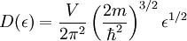
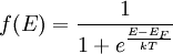
Band structures in different types of solidsAlthough electronic band structures are usually associated with crystalline materials, quasi-crystalline and amorphous solids may also exhibit band structures. However, the periodic nature and symmetrical properties of crystalline materials makes it much easier to examine the band structures of these materials theoretically. In addition, the well-defined symmetry axes of crystalline materials makes it possible to determine the dispersion relationship between the momentum (a 3-dimension vector quantity) and energy of a material. As a result, virtually all of the existing theoretical work on the electronic band structure of solids has focused on crystalline materials. Density of statesWhile the density of energy states in a band is very great, it is not uniform. It approaches zero at the band boundaries, and is generally greatest near the middle of a band. The density of states for the free electron model in three dimensions is given by, Filling of bandsAlthough the number of states in all of the bands is effectively infinite, in an uncharged material the number of electrons is equal only to the number of protons in the atoms of the material. Therefore not all of the states are occupied by electrons ("filled") at any time. The likelihood of any particular state being filled at any temperature is given by the Fermi-Dirac statistics. The probability is given by the following: where:
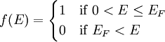
The Fermi level naturally is the level at which the electrons and protons are balanced. Regardless of the temperature, f(EF) = 1 / 2. At T=0, the distribution is a simple step function: At nonzero temperatures, the step "smooths out", so that an appreciable number of states below the Fermi level are empty, and some states above the Fermi level are filled. Band structure of crystalsBrillouin zoneBecause electron momentum is the reciprocal of space, the dispersion relation between the energy and momentum of electrons can best be described in reciprocal space. It turns out that for crystalline structures, the dispersion relation of the electrons is periodic, and that the Brillouin zone is the smallest repeating space within this periodic structure. For an infinitely large crystal, if the dispersion relation for an electron is defined throughout the Brillouin zone, then it is defined throughout the entire reciprocal space. Theory of band structures in crystalsThe ansatz is the special case of electron waves in a periodic crystal lattice using Bloch waves as treated generally in the dynamical theory of diffraction. Every crystal is a periodic structure which can be characterized by a Bravais lattice, and for each Bravais lattice we can determine the reciprocal lattice, which encapsulates the periodicity in a set of three reciprocal lattice vectors (
where From this theory, an attempt can be made to predict the band structure of a particular material, however most ab initio methods for electronic structure calculations fail to predict the observed band gap. Nearly-free electron approximationThe nearly-free electron approximation in solid state physics is similar in some respects to the hydrogen-like atom of quantum mechanics in that interactions between electrons are completely ignored. This allows use of Bloch's Theorem which states that electrons in a periodic potential have wavefunctions and energies which are periodic in wavevector up to a constant phase shift between neighboring reciprocal lattice vectors. The consequences of periodicity are described mathematically by the Bloch wavefunction: where the function
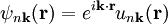
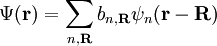
Here index n refers to the n-th energy band, wavevector k is related to the direction of motion of the electron, r is position in the crystal, and R is location of an atomic site. [1]. (For more detail see nearly-free electron model and pseudopotential method). Tight-binding modelThe opposite extreme to the nearly-free electron approximation assumes the electrons in the crystal behave much like an assembly of constituent atoms. This tight-binding model assumes the solution to the time-independent single electron Schrödinger equation Ψ is well approximated by a linear combination of atomic orbitals
where the coefficients
in which
Mott insulatorsAlthough the nearly-free electron approximation is able to describe many properties of electron band structures, one consequence of this theory is that it predicts the same number of electrons in each unit cell. If the number of electrons is odd, we would then expect that there is an unpaired electron in each unit cell, and thus that the valence band is not fully occupied, making the material a conductor. However, materials such as CoO that have an odd number of electrons per unit cell are insulators, in direct conflict with this result. This kind of material is known as a Mott insulator, and requires inclusion of detailed electron-electron interactions (treated only as an averaged effect on the crystal potential in band theory) to explain the discrepancy. The Hubbard model is an approximate theory that can include these interactions. OtherCalculating band structures is an important topic in theoretical solid state physics. In addition to the models mentioned above, other models include the following:
The band structure has been generalised to wavevectors that are complex numbers, resulting in what is called a complex band structure, which is of interest at surfaces and interfaces. Each model describes some types of solids very well, and others poorly. The nearly-free electron model works well for metals, but poorly for non-metals. The tight binding model is extremely accurate for ionic insulators, such as metal halide salts (e.g. NaCl). References
Further reading
See also
Categories: Condensed matter physics | Semiconductors |
|
| This article is licensed under the GNU Free Documentation License. It uses material from the Wikipedia article "Electronic_band_structure". A list of authors is available in Wikipedia. |


 ,
,
 ,
,  ,
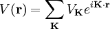
,  ). Now, any periodic potential
  which shares the same periodicity as the direct lattice can be expanded out as a Fourier series whose only non-vanishing components are those associated with the reciprocal lattice vectors. So the expansion can be written as:
 for any set of integers
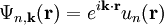
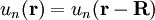
 is periodic over the crystal lattice, that is,
 .
.
 .
.
 ,
,
 are selected to give the best approximate solution of this form. Index n refers to an atomic energy level and R refers to an atomic site. A more accurate approach using this idea employs Wannier functions, defined by
 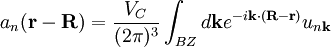 ;
;
 is the periodic part of the Bloch wave and the integral is over the
 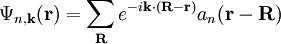 .
.
Last viewed


