Honouring the inventor who brought single atoms into focus
Maximilian Haider named European Inventor Award 2019 finalist
Advertisement


The European Patent Office (EPO) announces that Austrian experimental physicist and entrepreneur Maximilian Haider has been nominated for the European Inventor Award 2019 as one of three finalists in the category "Lifetime achievement" for his pioneering technique to improve the resolution of electron microscopes, one of the most widely used research tools in modern science. Thanks to his work over decades, electron microscope images are now five times sharper, enabling for instance researchers to view semiconductor crystals with atomic resolution. This insight has notably helped microchip manufacturers to reduce the scale of components found in mobile devices.
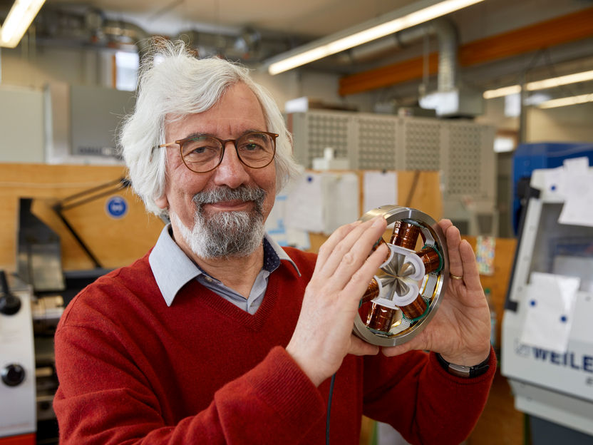
Maximilian Haider (Austria), nominated for the European Inventor Award 2019 in the category Lifetime achievement
European Patent Office
Haider – who is today Professor in Electron Optics at the Karlsruhe Institute of Technology, Germany – began commercialising his technology in 1996, co-founding his company Corrected Electron Optical Systems GmbH (CEOS) which dominates the market, designing corrective technology for global microscope manufacturers including Hitachi, JEOL and Thermo-Fisher Scientific.
"Haider's invention helped electron microscopes focus down to the atomic scale, which has in turn supported advances in materials sciences," said EPO President António Campinos about the Austrian's nomination. "For decades, his work and his company have been highly influential in the field of electron microscopy."

The winners of the 2019 edition of the EPO's annual innovation prize will be announced at a ceremony in Vienna on 20 June.
Building the first electronic lens
Since their introduction more than 60 years ago, electron microscopes have grown into one of the most commonly used tools by researchers around the globe. By channelling beams of electrons instead of light, they can reveal objects too small to observe with optical microscopes. Up until 20 years ago, the beams of charged particles operating inside these instruments gave rise to image deformations that limited their resolution. A theory of how this problem could be solved, by the German physicist Otto Scherzer, had existed since the 1940s but had not been successfully put to the test due to the limitations of technology at the time. This situation was to remain until Austrian experimental physicist Maximilian Haider put a solution into practice in the 1990s.
Born in Freistadt, Austria, in 1950, Haider had an early interest in lenses and resolution as he worked in his teens as an apprentice with opticians in Linz and Cologne before returning to formal education as an adult, and obtaining a high school diploma at the age of 26. He then studied physics at Kiel University and Darmstadt Technical University in Germany, where he met German theoretical physicist Harald Rose who convinced him to move away from light optics and pursue a PhD on overcoming the resolution limit of electron microscopy.
Over the following years, Haider worked with Rose and German material scientist Kurt Urban on potential solutions to electron beam distortion. Haider's role was to put these concepts into practice by exploring the electronic components needed to correct this distortion. Upon completing his PhD in 1987, Haider joined the European Molecular Biology Laboratory (EMBL) in Heidelberg, where he later led the Electron Microscopy Group and continued his work on corrective technology.
The technology he developed is a set of magnetic pole-pieces (known as hexapoles and lenses) that bend beams of charged particle inside electron microscopes to compensate for their inherent distortions and reduce the blur in their images. Haider compares the invention to an optical lens that corrects a person's eyesight by focussing images on the retina. In the same way, the electrodes cancel out the distortions that arise within charged particle beams on their way from the sample to the detector.
In 1996, Haider cofounded, together with Rose and German physicist Joachim Zach – who also studied under Rose at the Technical University of Darmstadt and worked with Haider at EMBL – CEOS. The company, based in Heidelberg Germany, began working with world leading microscope suppliers to commercialise Haider's technology.
The following year, as funding for his research at EMBL came close to running out, Haider and his partners finally got the technology operational, achieving a record resolution of just 0.12 nanometres with an electron microscope and enabling material scientists to identify, for the first time, single atomic layers in semiconductor crystals. This invention notably proved beneficial to manufacturers of microchips as it made it possible to visualise increasingly small features and defects on components for computers and later smartphones.
'It was a real breakthrough for science and electron optics and for all the material scientists because of the high resolution we could now offer, ' says Haider.
Haider applied for a patent in 1998 to protect the technology he had nurtured since his PhD and took it to the market with CEOS-partner JEOL. 'What we patented were the details of how to bring the concept into practice and to make it appropriate for users, ' he said.
CEOS also commercialised an electronic beam corrector with Philips. After Haider and colleagues published a landmark paper on their invention in Nature, other suppliers of electron microscopes including Hitachi wanted the start-up to provide them with their corrector. Haider has since been granted 10 European patents for inventions that have further improved the resolution of electron microscopy and extended its applications. In 2015, his work notably permitted world-record resolutions of 0.043 nanometres, which is shorter than the radius of a hydrogen-atom.
Driving advances in high resolution
CEOS is today a market leader in correction technology and precision equipment for electronic microscopes with 47 employees and over a million euros in annual profits. The company provides components for 90% of all transmission electron microscopes on the market today, working with leading microscope suppliers including JEOL, Philips, Hitachi, Thermo Fisher Scientific and ZEISS to continually push the limits of their technology so that researchers can benefit from even sharper, improved images.
The advances in electron imaging brought by Haider's invention have pushed back the horizon of what can be visualised by researchers in countless disciplines in physics, chemistry and the life sciences. The ability to focus down to the atomic scale with precision has meant that they have been able to create new materials for new applications. For the last 20 years, Haider's work has therefore supported the boom in nanotechnology, notably in monitoring the structure and defects as microelectronic manufacturers miniaturise components for computers and smartphones, and has found applications in fields including solar cells and batteries.
With the transmission electron microscope market worth EUR 550 million in 2016 and expected to grow to EUR 650 million by 2021, CEOS is building on the success of its founder and working with partners to drive further advances in the field.
For Haider, his lifetime achievement is both his invention, contributing to advances in electron microscopy, and the company he helped grow and which he continues to support as a senior advisor.


Other news from the department science


