Perovskite Solar Cells: paving the way for rational ink design for industrial-scale manufacturing
Advertisement


For the production of high-quality metal-halide perovskite thin-films for large area photovoltaic modules often optimized inks are used which contain a mixture of solvents. An HZB team at BESSY II has now analysed the crystallisation processes within such mixtures. A model has also been developed to assess the kinetics of the crystallisation processes for different solvent mixtures. The results are of high importance for the further development of perovskite inks for industrial-scale deposition processes of these semiconductors.
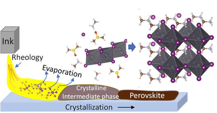
Schematic illustration: the solvants (ink) are used to produce a thin film of polycrystalline perovskite.
© HZB
Hybrid organic perovskite semiconductors are a class of materials for solar cells, which promise high efficiencies at low costs. They can be processed from precursor solutions that upon evaporation on a substrate form a polycrystalline thin film. Simple manufacturing processes, such as spin coating a precursor solution, often only lead to good results on a laboratory scale, i.e. for very small samples.
Printing large areas
For the production of larger area photovoltaic modules, the team of Dr. Eva Unger develops printing and coating processes in which the perovskite semiconductor is processed from inks containing the precursors dissolved in solvents. The composition of the ink determines the material formation mechanism with the solvent affecting the process by its rheological properties, evaporation rate and participation in intermediate phases. "Our research question in this project was: How can we rationalize the difference in crystallization kinetics when using different solvents," explains Unger, who heads the Young Investigator Group Hybrid Materials Formation and Scaling.
Different evaporation rates
In solvents with only one component, the crystallization process is determined by the evaporation rate. "In mixtures of solvents, evaporation is dominated by the most volatile component that evaporates the fastest. This changes the ratio of solvents that are present upon crystallization", says Dr. Oleksandra Shargaieva, postdoc in Unger's team.
Crystallization analyzed at BESSY II
At the KMC-2 beamline of BESSY II, she was able to analyse the formation of the perovskite semiconductor and crystalline intermediate phases incorporating solvent molecules during the evaporation of the solvents. “I found that the formation mechanism critically depends both on the solvents evaporation rate and binding strength to the lead-halide. “These insights will help to predict the kinetics of crystallization processes of the perovskite thin film for different solvent combinations based on the properties of the precursor solutions”, says Shargaieva.
"There is still a lack of systematic knowledge when scaling up from laboratory scale to industrial area sizes. With these results we pave the way for further ink design to enable industrial-scale manufacturing or perovskite thin films of high quality”, says Unger.
Original publication


Other news from the department science


Most read news


More news from our other portals


Last viewed contents
What is the origin of the visible mass of the universe? - Supercomputer calculates the mass of the nucleon
Dow Canada Finalizes Sale of Western Canada Caustic Soda Business to Univar
