Focused ion beam technology: a single tool for a wide range of applications
From physics, materials science and chemistry to life sciences and even archaeology
Advertisement


Processing materials on the nanoscale, producing prototypes for microelectronics or analysing biological samples: The range of applications for finely focused ion beams is huge. Experts from the EU collaboration FIT4NANO have now reviewed the many options and developed a roadmap for the future. The article, published in “Applied Physics Review” is aimed at students, users from industry and science as well as research policy makers.
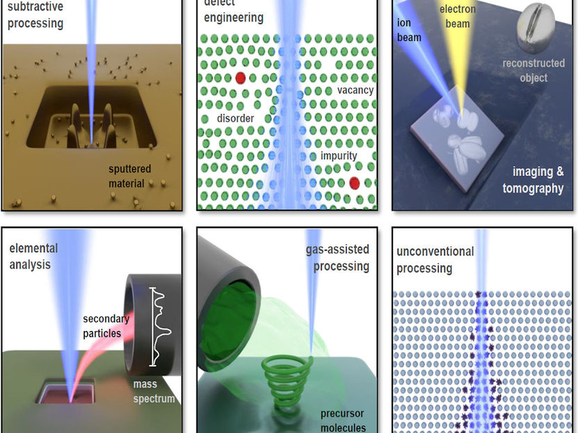
Focused ion beams can be used to analyse, structure or optimise materials - enabling a wide range of possible applications. The publication from the Fit4Nano project provides an overview and a roadmap for future developments.
N. Klingner/HZDR, Katja Höflich/HZB
“We realized that focused ion beams can be used in many different ways, and we thought we had a good overview at the start of the project. But then we discovered that there are many more applications than we thought. In many publications, the use of focused ion beams is not even explicitly mentioned, but is hidden in the methods section. It was detective work,” says Dr Katja Höflich, physicist at the Ferdinand-Braun-Institut and the Helmholtz-Zentrum Berlin (HZB), who coordinated the comprehensive report. “In particular, we found work from the 1960s and 1970s that was ahead of its time and unjustly forgotten. They still provide important insights today”.
The report provides an overview of the current state of focused ion beam (FIB) technology, its applications with many examples, the most important equipment developments and future prospects. “We wanted to provide a reference work that is useful for academic research and industrial R&D departments, but also helps research management to find their way in this field,” says Dr Gregor Hlawacek, group leader at the Institute of Ion Beam Physics and Materials Research at Helmholtz-Zentrum Dresden-Rossendorf (HZDR). Hlawacek leads the FIT4NANO project, an EU project on FIB technologies, in which the authors of the report are involved.
From basic research to the finished component
FIB instruments use a focused ion beam of typically two to 30 keV. With its small diameter in the nanometre and sub-nanometre range, such an ion beam scans the sample and can change its surface with nanometre precision. FIB instruments are a universal tool for analysis, maskless local material modification and rapid prototyping of microelectronic components. The first FIB instruments were used in the semiconductor industry to correct photomasks with focused gallium ions. Today, FIB instruments are available with many different types of ions. An important application is the preparation of samples for high-resolution, nanometre-precision imaging in the electron microscope. FIB methods have also been used in the life sciences, for example to analyse and image micro-organisms and viruses with FIB-based tomography, providing deep insights into microscopic structures and their function.
FIB instruments are constantly evolving towards other energies, heavier ions and new capabilities, such as the spatially resolved generation of single atomic defects in otherwise perfect crystals. Such FIB processing of materials and components has enormous potential in quantum and information technology. The range of applications, from fundamental research to the finished device, from physics, materials science and chemistry to life sciences and even archaeology, is absolutely unique. “We hope that this roadmap will inspire scientific and technological breakthroughs and act as an incubator for future developments,” says Gregor Hlawacek.
Original publication


Other news from the department science


