Atomic switches: Ionic computing
Advertisement
A review of new types of nanodevices and computing based on cationic-based atomic switches is presented Takami Hino and coworkers at the WPI Center for Materials Nanoarchitectonics at the National Institute for Materials Science (NIMS) in Tsukuba, Japan. The review paper is published in Science and Technology of Advanced Materials.
The researchers describe the fundamental mechanisms governing the operation of nanoionic atomic switches with detailed examples of their own three terminal devices, and predict a bright future for integrating atomic switches with conventional silicon devices by using ionic conductive materials.
Mechanical atomic switches — operated by manipulating atoms between a conducting surface and the tip of a scanning tunneling microscope (STM) — were first reported in the early 1990s. These mechanical switches triggered intense interest in the development of electrically controlled atomic switches, produced by the movement of cationic ions in solid electrochemical reactions, where the operation of cationic atomic switches is governed by the formation of a conducting channel either in or on an ionic conductor.
Now, the challenge for researchers in this field is the fabrication of nanoionic device structures that can be integrated with conventional metal oxide silicon semiconductor devices.
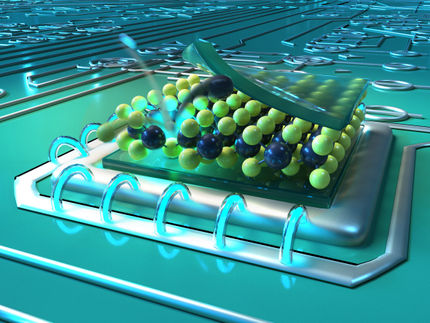
In its simplest configuration, the operation of a nanoionic atomic switch consists of the formation and disintegration of nanometer sized metallic wires via a solid electrochemical reaction, which leads to major changes in the resistance between electrodes—the ‘on’ and ‘off’ states.
In this review, Hino and colleagues describe the control of silver ions in silver sulphide — an ionic conductor — using an STM tip to inject electrons to produce silver protrusions on the surface of silver sulphide, and their shrinkage by applying an appropriate bias voltage between the STM tip and electrode. Importantly, the application of a positive bias between a silver sulphide tip and a platinum surface leads to the growth of silver wires and a negative bias led their shrinkage. This bipolar control is important for practical device applications.
Gap-type atomic switches are a fundamental building block for bipolar nanoionic devices. Here, the researchers give a detailed account of bipolar switching using silver sulphide STM tips and platinum electrodes based on their own experiments on ‘crossbar’ device structures with a 1 nm gap between silver sulphide and platinum, with emphasis on the physical mechanism governing high speed switching at 1 MHz, and the finding that switching time decreases exponentially with increasing bias voltage. The authors stress that the development of a reproducible method for fabricating ‘crossbar’ devices was a major breakthrough, which enabled the first demonstration of nanoionic circuits such as logic gates.
With a view to practical applications of atomic switches, the authors give examples of advanced atomic switches including gapless-type devices consisting of metal/ionic conductor/metal structures, where one of the metals is electrochemically active and the other inert. Notably, recent reports on the use of metal oxides as ionic conductors have added further momentum for device commercialization.
Notably, gapless atomic switches also act as so-called ‘memristors’ (memory resistors) — passive two terminal multi-state memory devices — where the size of the nanowire protrusion governs the operation characteristics.
Other advanced atomic switches include: three terminal devices such as structures with a solid copper sulphide electrolyte, where the formation of a copper bridge between a platinum-source electrode and copper-drain electrode is controlled by a copper gate-electrode; and photoassisted atomic switches, which do not require nanogaps, and nanowire protrusions are grown by optical irradiation of a photoconductive material located between the anion and electron conducting electrode and a counter metal electrode. Intriguingly, since the switch is turned ‘on’ when the growing metal protrusion reaches the counter electrode, and the protrusion does not grow in the dark, the photoassisted atomic switch behaves as a programmable switch that could be used in erasable programmable read-only memory (EPROM).
The authors also describe the ‘learning abilities’ of atomic switches capable of short-term and long-term memories in single nanoionic devices; nonvolatile bipolar switches; two terminal atomic switch logic gates; and field programmable gate arrays integrated with CMOS devices.
Original publication
Takami Hino et al, "Atomic switches: atomic-movement-controlled nanodevices for new types of computing,"; Sci. Technol. Adv. Mater.12 (2011) 013003.


