Order in the disorder: density fluctuations in amorphous silicon discovered
New study shows that three different phases form within the amorphous matrix, which influences the quality and lifetime of the semiconductor layer
Advertisement


For the first time, a team at HZB has identified the atomic substructure of amorphous silicon with a resolution of 0.8 nanometres using X-ray and neutron scattering at BESSY II and BER II. Such a-Si:H thin films have been used for decades in solar cells, TFT displays, and detectors. The results show that three different phases form within the amorphous matrix, which dramatically influences the quality and lifetime of the semiconductor layer.
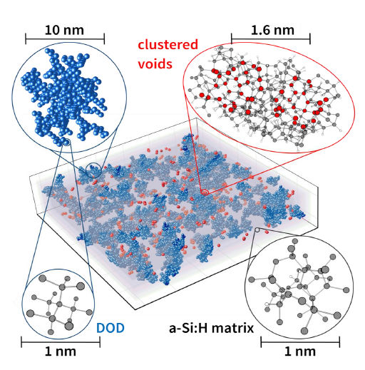
Structural model of highly porous a-Si:H, which was deposited very quickly, calculated based on measurement data. Densely ordered domains (DOD) are drawn in blue and cavities in red. The grey layer represents the disordered a-Si:H matrix. The round sections show the nanostructures enlarged to atomic resolution (below, Si atoms: grey, Si atoms on the surfaces of the voids: red; H: white)
© Eike Gericke/HZB
Silicon does not have to be crystalline, but can also be produced as an amorphous thin film. In such amorphous films, the atomic structure is disordered like in a liquid or glass. If additional hydrogen is incorporated during the production of these thin layers, so-called a-Si:H layers are formed. "Such a-Si:H thin films have been known for decades and are used for various applications, for example as contact layers in world record tandem solar cells made of perovskite and silicon, recently developed by HZB" explains Prof. Klaus Lips from HZB. "With this study, we show that the a-Si:H is by no means a homogeneously amorphous material. The amorphous matrix is interspersed with nanometre-sized areas of varying local density, from cavities to areas of extremely high order," the physicist comments.
Order on the nanoscale
In cooperation with the Technical Universities of Eindhoven and Delft, Lips and his team have succeeded for the first time in experimentally observing and quantitatively measuring these inhomogeneities in differently produced a-Si:H thin films. To do this, they combined the results of complementary analytical methods to form an overall picture.
Experiments at BESSY II, BER II and Corelabs
"We find a nanoscopic order in the disorder of the a-Si:H layers by x-ray scattering measurements performed at BESSY II. We were then able to determine the distribution of the hydrogen atoms in the amorphous network by neutron scattering at the former research reactor BER II at the HZB site Wannsee", says Eike Gericke, PhD student and first author of the paper. Further insights were provided by the electron microscopy performed at the CCMS Corelab and measurements of electron spin resonance (ESR).
Clusters of voids
"We were able to discover nanometer-sized voids, which are created by slightly more than 10 missing atoms. These voids arrange themselves into clusters with a recurrent distance of about 1.6 nanometres to each other," explains Gericke. These voids are found in increased concentrations when the a-Si:H layer has been deposited at a very high rate.
Islands of higher order
The researchers also found nanometre-sized regions with higher order compared to the surrounding disordered material. These densely ordered domains (DOD) contain hardly any hydrogen. "The DODs form aggregates of up to 15 nanometres in diameter and are found in all the a-Si:H materials considered here," explains Gericke.
"The DOD regions have been theoretically predicted in 2012* and are able to reduce mechanical stress in the material and thus contribute to the stability of the a-Si:H thin film. The voids on the other hand, can promote electronic degradation of the semiconductor layers as indicated by ESR measurements," says Klaus Lips.
New applications in sight
Targeted optimization of manufacturing processes with regard to the substructures now discovered could enable new applications such as optical waveguides for programmable photonic systems or a future silicon battery technology. Last but not least, the findings will also help to finally unravel the microscopic mechanism of light-induced degradation of a-Si:H solar cells, one of the puzzles the scientific community is trying to solve since more than 40 years.
Original publication


Other news from the department science


