When Material Defects Become Energy Carriers
Researchers in Kiel Discover a New Mechanism for Energy Transport in Atomically Thin Materials
Advertisement


Atomic defects are inevitable: No material is completely free of defects. However, what was long considered primarily a weakness could also be a strength. Researchers at Christian-Albrechts-University of Kiel (CAU) have now shown that such defects can not only absorb energy but also selectively transmit it. A team led by Nahid Talebi, professor of nanooptics at CAU, recently published a study on this topic in the journal ACS Nano.
Defects Form a Network
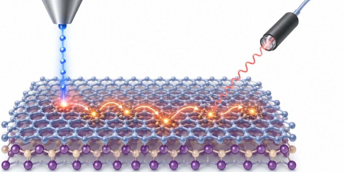
How energy transport works is demonstrated by the interaction of two materials that are only a few atomic layers thick: a perovskite that can absorb energy, and hexagonal boron nitride. The latter class of materials consists of boron and nitrogen atoms that are normally arranged in a regular pattern. However, some sites deviate from this structure. These atomic defects can absorb energy from the perovskite and pass it on to other defects. The energy in the perovskite initially exists in an excited state, which physicists call an exciton. The team assumes that the energy is transferred from these states to defects in the boron nitride.
The extent to which the energy can propagate through this network of defects is remarkable: the team was able to detect the signal even at a distance of up to 150 micrometers from the original site of excitation. This corresponds roughly to the width of a human hair. The measured energy transport length was approximately 142 micrometers.
According to the experiments, conventional approaches—such as the movement of excitons alone or an optical waveguide—are insufficient to explain this distance. The researchers attribute the observed energy transport primarily to the interactions between the defects and to the repeated absorption and emission of light within the defect network.
Crucial to the discovery was a specialized cathodoluminescence measurement method developed by the Kiel nano-optics team. In this process, the researchers excited the material with an electron beam and detected the resulting light using an optical fiber. The electron beam remained at the same location throughout the experiment, while they gradually moved the fiber away from it. At the same time, they observed what was happening under an electron microscope and found that the light signal was still present even at a great distance from the excitation site.
New Possibilities for Optical and Quantum Technologies
“Many quantum materials normally need to be cooled so that we can observe their properties at all. Our effect, however, occurs at room temperature. That makes it particularly exciting to investigate further,” says Talebi, a member of the KiNSIS research cluster—Kiel Nano, Surface, and Interface Science. There, scientists are researching, among other things, nanoscale materials and interfaces for applications in quantum technology. The team also sees potential for new devices in which energy or information is transported via light-induced excitations.
Next, the researchers want to find out how they can specifically control the energy exchange in the material under investigation. Talebi hopes that this will advance the development of hybrid quantum materials. The paper first lays out the physical foundations for this and cites, for example, quantum transducers—which transmit quantum information between different systems—and optoelectronic connections for high-speed data transmission as potential applications.
Note: This article has been translated using a computer system without human intervention. LUMITOS offers these automatic translations to present a wider range of current news. Since this article has been translated with automatic translation, it is possible that it contains errors in vocabulary, syntax or grammar. The original article in German can be found here.
Original publication


Other news from the department science